Introduction
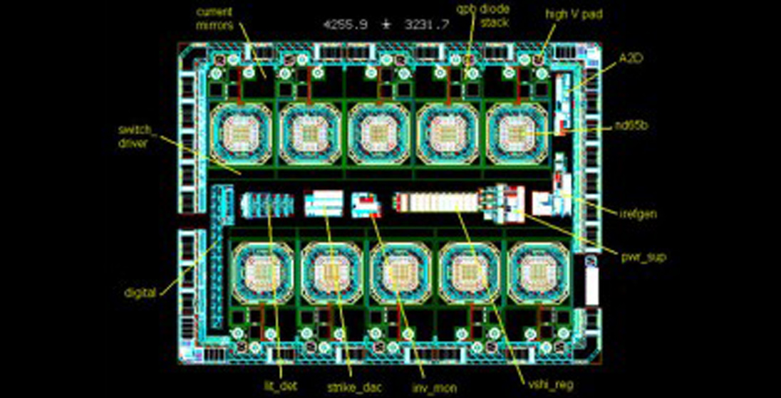
This project consisted of a design and development of a power control integrated circuit. The IC contained analog and digital circuits, an analog to digital converter, voltage reference, control interface and 10 high voltage MOSFETs, which were placed in isolation wells within the IC substrate.
Customer Objectives
- Capability to switch AC voltages >600 Volts to a set of loads
- IC development completion in < 9 months
- 10 Loads
- Analog to digital conversion immune to system noise
- Digital control interface
- Control the power delivered to the loads
- Minimal chip size
Results
A design team was assembled, the appropriate foundry and IC technology were chosen, and the analog parts of the chip were designed using circuit theory. Models for performance of various sections were developed and extensive simulations were carried out to ensure needed performance was obtained. Numerous design reviews were held during transistor level design and layout to minimize errors. A chip hardware emulator was concurrently designed and built to verify performance in the product of the future chip. Also, concurrently, test beds for testing the chip and reference designs for marketing purposes were developed.
As a result, the chip was completed on schedule in less than 9 months with zero design errors; successfully performed in various systems which were presented to customers. The price was competitive and satisfied the customer needs.


